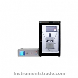
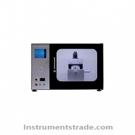
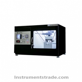
Introduction: Multi-mode AFM has a wide range of applications, including: Material science: observing and studying material surfaces, including surface roughness and surface structure, particle size, and defects; Microelectronics: On-line detection of large-scale integrated circuits, studying the local electrical characteristics of ICs, and being used for information storage and reading of ultra-high-density (100 million times that of current disks) Biology: DNA, chromatin structure, protein/enzyme reactions, protein adsorption, etc. Medicine: a powerful means of mesoscopic operation, its application areas involve medicine, pharmacology, immunity, diagnosis and treatment and other disciplines Optics: The combination of optical technology and AFM technology can form a new discipline; near-field optics, which combines the unparalleled resolution of AFM technology in detecting topography with the advantages of optical field observations. Physics: AFM can detect the surface's electronic structure, energy level, wave function, tunneling effect and so on. Mesoscopic physics studies can be conducted to study the interaction of electrons with adsorbed atoms Chemistry: AFM can be used as an effective in-situ detection tool to study surface chemical reactions at the atomic level. It can also observe atomic-level changes in surface chemical reactions. Features: 1. Miniaturized and detachable design, easy to carry and teaching; 2. Laser detection head and sample scanning stand integrated, stable and reliable; 3. Precision laser and probe positioning device, replacement of probes and adjustment of light spot is simple and convenient; 4. The uniaxially driven sample automatically approaches the probe vertically and accurately positions the scanning area so that the tip is scanned perpendicular to the sample; 5. Motor control pressure electric ceramic automatic detection of intelligent needles, protection probes and samples; 6. 4X objective optical positioning, without focusing, real-time observation and positioning probe sample scanning area; 7. Spring suspension type shockproof method, simple and practical, good shockproof effect; 8. Integrated scanner hardware nonlinear correction user editor, Nano characterization and measurement accuracy is better than 98%. Technical Parameters Basic operating modes: tapping mode, RMS-Z curve measurement Optional work modes: contact mode, F-Z force curve measurement, friction/side force, amplitude/phase, magnetic force and electrostatic force Sample size: Φ ≤ 90mm, H ≤ 20mm Scan range: XY to 20um, Z to 2um Scanning resolution: XY to 0.2nm, Z to 0.05nm Sample movement range: 0~13mm Optical magnification 4X, optical resolution 2.5um Scan rate 0.6Hz~4.34Hz, scan angle 0~360° Scan Control: XY uses 18-bit D/A, Z uses 16-bit D/A Data sampling: 14-bit A/D, dual 16-bit A/D multiplex simultaneous sampling Feedback method: DSP digital feedback Feedback sampling rate: 64.0KHz Communication interface: USB2.0/3.0 Operating environment: WindowsXP/7/8/10 operating system
Introduction: Multi-mode AFM has a wide range of applications, including: Material science: observing and studying material surfaces, including surface roughness and surface structure, particle size, and defects; Microelectronics: On-line detection of large-scale integrated circuits, studying the local electrical characteristics of ICs, and being used for information storage and reading of ultra-high-density (100 million times that of current disks) Biology: DNA, chromatin structure, protein/enzyme reactions, protein adsorption, etc. Medicine: a powerful means of mesoscopic operation, its application areas involve medicine, pharmacology, immunity, diagnosis and treatment and other disciplines Optics: The combination of optical technology and AFM technology can form a new discipline; near-field optics, which combines the unparalleled resolution of AFM technology in detecting topography with the advantages of optical field observations. Physics: AFM can detect the surface's electronic structure, energy level, wave function, tunneling effect and so on. Mesoscopic physics studies can be conducted to study the interaction of electrons with adsorbed atoms Chemistry: AFM can be used as an effective in-situ detection tool to study surface chemical reactions at the atomic level. It can also observe atomic-level changes in surface chemical reactions.